Tesla's Terafab: In-House AI Chip Foundry Launches March 21
On March 14, Elon Musk posted seven words on X: "Terafab Project launches in 7 days." The post drew 77,000 likes and 8,000 retweets within hours, signaling that Tesla's most ambitious infrastructure bet is entering its next phase.
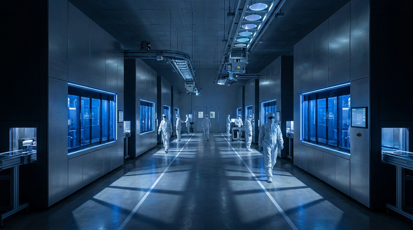
What Terafab Is
Terafab is Tesla's planned in-house semiconductor fabrication facility, first disclosed on the company's January 28 earnings call. Unlike conventional chip designers that outsource manufacturing to TSMC or Samsung, Tesla intends to vertically integrate logic processing, memory, and advanced packaging under one roof — at a scale no private company in North America currently operates.
The facility targets 2nm process technology with initial capacity of 100,000 wafer starts per month, scaling toward one million — roughly 70% of TSMC's entire current global output. Annual production is targeted at 100 to 200 billion custom AI and memory chips. Estimated construction cost is approximately $25 billion.
Who It's For
Tesla's own AI roadmap is the primary driver. Cybercab robotaxis, Optimus humanoid robots, and next-generation Full Self-Driving all require chip volumes that no external supplier can commit to on Tesla's timeline. Terafab is also expected to serve xAI's Grok model training infrastructure, making both companies independent from third-party foundries.
Tesla's fifth-generation chip, AI5, is the first product Terafab is designed to produce. Small-batch production is expected in 2026, with volume production projected for 2027.
What "Launch" Actually Means
A fully operational fab won't open March 21 — semiconductor facilities take years to build and commission. The announcement most likely signals a groundbreaking ceremony, site reveal, or formal disclosure of construction partners and build timeline. Musk has previously discussed potential collaboration with Intel on the project.